E-mail: cysi@cysi.wang

")
")

PECVD equipment uses the principle of flat plate capacitive glow discharge to dissociate the process gas passing into the deposition chamber and generate plasma. The dissociated groups re-react chemically in the plasma. Due to the presence of plasma, the decomposition

Using plasma enhanced chemical vapor deposition technology, low basic temperature, fast deposition rate, deposition of silicon nitride, amorphous silicon and microcrystalline silicon films on optical glass, silicon, quartz, stainless steel and other substrate materials, good film forming quality, fewer pinholes, not easy to crack, suitable for the preparation of amorphous silicon and microcrystalline silicon thin film solar cell devices. It can be widely used in the research and small batch preparation of thin film materials in colleges and universities and research institutes.
PECVD equipment uses the principle of flat plate capacitive glow discharge to dissociate the process gas passing into the deposition chamber and generate plasma. The dissociated groups re-react chemically in the plasma. Due to the presence of plasma, the decomposition, combination, excitation and ionization of gas molecules are promoted, and the formation of reactive groups is promoted, thus reducing the deposition temperature. A film is deposited on a substrate at a certain temperature. The density and energy of the plasma can be adjusted according to the process, and the growth rate and microstructure of the film can be controlled.
If you are interested in our evaporation coater, please contact us for more information.
Tel:138 3857 9492
Email:carol@cysitech.com
Contact:Carol Xu
Wechat:15290599353
WhatsApp/Skype: 13838579492
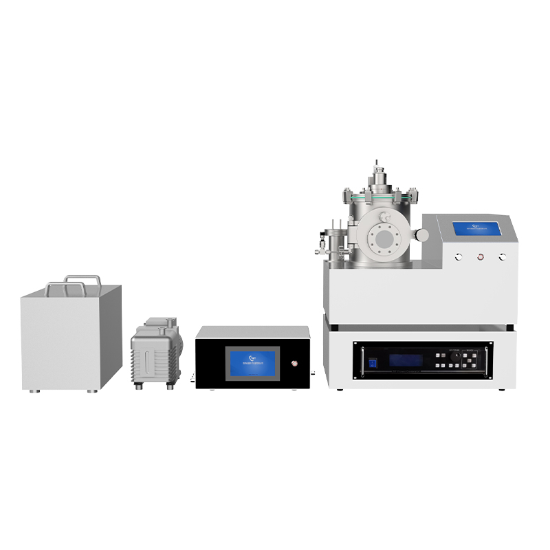
Product name | Tabletop 4-inch Flat Plate Plasma Enhanced Chemical Vapor Deposition (PECVD) | |
Product model | CY-PECVD-240T-SS | |
Input power supply | AC220V 50Hz | |
RF power supply | Signal frequency | 13.56MHz |
Power output range | 0~500W (can choose 150W, 300W, 1000W, etc) | |
Working chamber | Heating temperature | RT-500℃ (can choose 600℃, 800℃, 1000℃, etc.) |
Sample holder size | Φ100mm (Compatible with samples 4 inches and below) | |
Rotating speed of sample holder | 1-20rpm adjustable | |
Chamber material | Stainless steel | |
Observation window | Φ60mm, with baffle | |
Gas supply system | Channel numbers | 3 (Other channels, other gas types, and other measurement ranges can be selected as required) |
Measuring unit | Mass flow controller | |
Measuring range | A channel: 0~200SCCM for O2 | |
B channel: 0~200SCCM for N2 | ||
C channel: 0~200SCCM for Ar | ||
Vacuum system | Backing pump | 1.1L/s |
Molecular pump | 60L/s | |
Vacuum measurement | Compound vacuum gauge | |
Vacuum degree | 5.0*10-3Pa | |
Water chiller | Water flow | 10L/min |
Cooling power | 50W/℃ | |
Part name | Description |
Main unit | 1 set, front door open, easy to take materials and samples |
Vacuum system | 1 set, providing a high vacuum environment, eliminates impurities in the cavity |
Gas supply system | 1 set, MFC |
Water chiller | 1 set, Circulating water cooling |
Accessories | Provided according to the specific configuration such as the clamp, bellows, water pipes and so on |
Manual | Paper English/Chinese manual or electronic version |
Application:
Semiconductor industry: In integrated circuit manufacturing, PECVD is one of the key technologies for manufacturing dielectrics, and is used to deposit thin films such as silicon dioxide and silicon nitride to isolate conductive layers and capacitors.
Photovoltaic field: In solar cell manufacturing, PECVD can uniformly deposit thin films on a wide surface area to improve the photoelectric conversion efficiency of solar cells.
Optical field: Used to produce coatings with specific optical properties, such as anti-reflective coatings and anti-reflective coatings, to improve the optical performance and service life of products.
Consumer electronics field: In the preparation of nanofilms, PECVD polymerized nanofilms have the advantages of uniform film thickness, high temperature resistance, wear resistance, and high purity, and are used for internal circuit boards of consumer electronic products.
New energy vehicle field: Used for the protection of key components of new energy vehicles, such as central control systems, boost charging systems, and BMS systems, to improve the stability and safety of the system.
Biomedical field: The dense inert coating produced by PECVD technology has excellent biocompatibility and corrosion resistance, and is used for surface modification of medical implants.
Tribology: Deposition of wear-resistant coatings such as diamond-like carbon (DLC) significantly improves the wear resistance and low friction of materials, and is used in mechanical parts, bearings, sliding parts, etc.
Other fields: Including food packaging materials, used to protect food from external pollutants and moisture, and to protect components and motherboards in harsh industrial environments.
Application case: Deposition of microcrystalline silicon (μc-Si) and amorphous silicon (a-Si) thin films using PECVD technology in solar cell
Experimental preparation
1. Clean the substrate:
Select a suitable substrate material, such as glass, ITO (indium tin oxide) glass or stainless steel substrate. Ensure that the substrate surface is free of dust, oil and other impurities.
Perform ultrasonic cleaning, use solvents such as acetone and isopropyl alcohol to clean, then rinse with deionized water, and finally dry.
2. Equipment preparation:
Ensure that the inside of the vacuum chamber of the PECVD system is clean and free of pollution.
Set up gas passages to ensure that the reaction gas (such as silane (SiH4), hydrogen (H2), etc.) is sufficient and the purity meets the requirements.
Set the RF power supply parameters according to the experimental requirements to ensure that the plasma can be stably generated.
Experimental operation:
1. Load the substrate:
Load the cleaned substrate onto the sample stage of the PECVD equipment, ensuring that the substrate surface is facing up and fixed in place.
Start the vacuum system and reduce the chamber pressure to about 10^-6 Torr to remove impurity gases in the chamber.
2. Preheat the substrate:
Start the substrate heating system and heat the substrate to the required deposition temperature. For microcrystalline silicon films, the temperature is usually between 200°C and 300°C; for amorphous silicon films, the temperature is usually between 150°C and 250°C.
Keep the temperature stable to ensure the quality of the film during the deposition process.
3. Gas flow setting:
According to the type of film (microcrystalline silicon or amorphous silicon), set the appropriate gas flow. Usually a mixture of silane (SiH4) and hydrogen (H2) is used to deposit silicon films. The proportion of hydrogen is higher when microcrystalline silicon is deposited, and the proportion of silane is higher when amorphous silicon is deposited.
The flow rate of each gas is accurately controlled by a mass flow controller (MFC).
4. Plasma generation:
Start the RF power supply to generate plasma. Usually the RF power is set between tens of watts and hundreds of watts, depending on the required film properties.
Control the power and frequency of the plasma to adjust the nucleation and growth rate of the film to ensure the uniformity of the film and the required crystal structure.
5. Deposition process:
Start film deposition under controlled gas flow and plasma conditions. The deposition time depends on the thickness of the required film, which usually ranges from tens of minutes to hours.
The film thickness is monitored in real time by online monitoring (such as ellipsometer or optical interferometry) to ensure that the required thickness is achieved (the thickness of microcrystalline silicon and amorphous silicon films is usually between hundreds of nanometers and several microns).
6. Termination of deposition:
After the required film thickness is achieved, turn off the gas flow and RF power to terminate the deposition process.
Continue to maintain the vacuum for a period of time to remove the residual gas in the chamber.
7. Cooling and unloading:
After the required film thickness is achieved, turn off the gas flow and RF power to terminate the deposition process.
Continue to maintain the vacuum for a period of time to remove the residual gas in the chamber.
Post-processing and characterization:
1. Film characterization:
Use X-ray diffraction (XRD), scanning electron microscopy (SEM), ellipsometer and other means to characterize the crystal structure, thickness and surface morphology of the film.
Evaluate the performance of the deposited film by measuring parameters such as the photoelectric conversion efficiency and minority carrier lifetime of solar cells.
2. Cell production:
If the film performance meets the requirements, the subsequent solar cell manufacturing steps can be carried out, such as electrode deposition, packaging, etc.
End of the experiment
Equipment cleaning:
After the experiment is completed, clean the PECVD equipment chamber to ensure that there is no residual sediment to prevent the impact on subsequent experiments.
Turn off the gas supply system to ensure that the equipment is in a safe state.
Through the above steps, high-quality microcrystalline silicon or amorphous silicon films can be successfully deposited on the substrate. These films play a vital role in thin-film solar cells and help improve the photoelectric conversion efficiency and stability of the cell.


Copyright © Zhengzhou CY Scientific Instrument Co., Ltd. All Rights Reserved Update cookies preferences
| Sitemap | Technical Support: 


")