E-mail: cysi@cysi.wang

")
")

plasma enhanced chemical vapor deposition technology suitable for the preparation of amorphous silicon and microcrystalline silicon thin film solar cell devices. It can be widely used in the research and small batch preparation of thin film materials in colleges and universities and research institutes

Using plasma enhanced chemical vapor deposition technology, low basic temperature, fast deposition rate, deposition of silicon nitride, amorphous silicon and microcrystalline silicon films on optical glass, silicon, quartz, stainless steel and other substrate materials, good film forming quality, fewer pinholes, not easy to crack, suitable for the preparation of amorphous silicon and microcrystalline silicon thin film solar cell devices. It can be widely used in the research and small batch preparation of thin film materials in colleges and universities and research institutes.
If you are interested in our evaporation coater, please contact us for more information.
Tel:138 3857 9492
Email:carol@cysitech.com
Contact:Carol Xu
Wechat:15290599353
WhatsApp/Skype: 13838579492
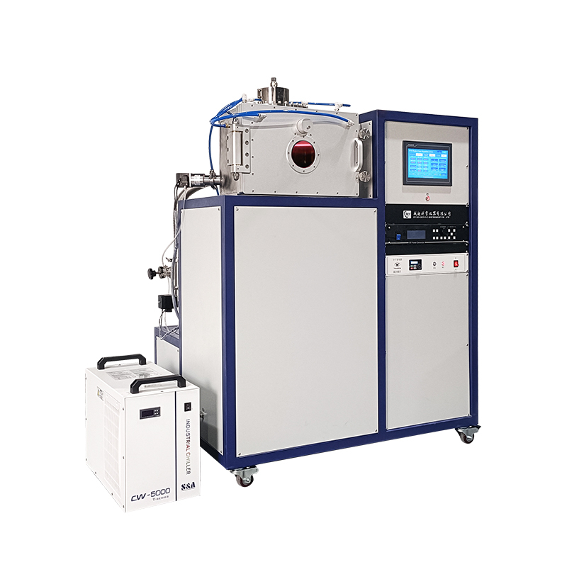
Product name | Floor-stand Flat Plate Plasma Enhanced Chemical Vapor Deposition (PECVD) | |
Product model | CY-PECVD-500T-SS | |
Input power supply | AC220V 50Hz | |
RF power supply | Signal frequency | 13.56MHz |
Power output range | 0~500W (can choose 150W, 300W, 1000W, etc) | |
Working chamber | Heating temperature | RT-500℃ (can choose 600℃, 800℃, 1000℃, etc.) |
Sample holder size | Φ200mm (Compatible with samples 8 inches and below) | |
Rotating speed of sample holder | 1-20rpm adjustable | |
Chamber material | Stainless steel | |
Observation window | Φ100mm, with baffle | |
Gas supply system | Channel numbers | 6 (Other channels, other gas types, and other measurement ranges can be selected as required) |
Measuring unit | Mass flow controller | |
Measuring range | ||
B channel: 0~200SCCM for CH4 | ||
C channel: 0~200SCCM for C2H4 | ||
D channel: 0~500SCCM for N2 | ||
E channel: 0~500SCCM for NH3 | ||
F channel: 0~500SCCM for Ar | ||
Vacuum system | Backing pump | 4.4L/s |
Molecular pump | 1200L/s | |
Vacuum measurement | Compound vacuum gauge | |
Vacuum degree | 5.0*10-3Pa | |
Water chiller | Water flow | 10L/min |
Cooling power | 50W/℃ | |
Part name | Description |
Main unit | 1 set, D-shape chamber, front door open, easy to take materials and samples |
Vacuum system | 1 set, providing a high vacuum environment, eliminates impurities in the cavity |
Gas supply system | 1 set, MFC |
Water chiller | 1 set, Circulating water cooling |
Air compressor | 1 set |
Accessories | Provided according to the specific configuration such as the clamp, bellows, water pipes and so on |
Manual | Paper English/Chinese manual or electronic version |
Semiconductor industry: In integrated circuit manufacturing, PECVD is one of the key technologies for manufacturing dielectrics, and is used to deposit thin films such as silicon dioxide and silicon nitride to isolate conductive layers and capacitors.
Photovoltaic field: In solar cell manufacturing, PECVD can uniformly deposit thin films on a wide surface area to improve the photoelectric conversion efficiency of solar cells.
Optical field: Used to produce coatings with specific optical properties, such as anti-reflective coatings and anti-reflective coatings, to improve the optical performance and service life of products.
Consumer electronics field: In the preparation of nanofilms, PECVD polymerized nanofilms have the advantages of uniform film thickness, high temperature resistance, wear resistance, and high purity, and are used for internal circuit boards of consumer electronic products.
New energy vehicle field: Used for the protection of key components of new energy vehicles, such as central control systems, boost charging systems, and BMS systems, to improve the stability and safety of the system.
Biomedical field: The dense inert coating produced by PECVD technology has excellent biocompatibility and corrosion resistance, and is used for surface modification of medical implants.
Tribology: Deposition of wear-resistant coatings such as diamond-like carbon (DLC) significantly improves the wear resistance and low friction of materials, and is used in mechanical parts, bearings, sliding parts, etc.
Other fields: Including food packaging materials, used to protect food from external pollutants and moisture, and to protect components and motherboards in harsh industrial environments.
Application Case: Deposition of passivation layers (such as silicon nitride (SiNx) or silicon oxide (SiO2) passivation layers) using PECVD technology in solar cell
Experimental preparation:
1. Clean substrate:
Select the silicon wafer to be deposited as the substrate. Silicon wafers are usually cut, polished, cleaned and pre-treated.
Use standard cleaning procedures (such as RCA cleaning) to remove organic pollutants and oxide layers on the surface of the silicon wafer to ensure that the deposited material is well bonded to the substrate.
2. Equipment preparation:
Check the vacuum chamber of the PECVD system to ensure that the inside of the chamber is clean and free of pollution.
Set up the gas passage to ensure that the gases required for the experiment (such as silane (SiH4), ammonia (NH3), oxygen (O2), etc.) are sufficient and the purity meets the requirements.
Set and adjust the RF power supply according to the experimental requirements to ensure that the plasma can be generated stably.
Experimental operation:
1. Load the substrate:
Load the cleaned silicon wafer onto the sample stage of the PECVD equipment, ensuring that the surface of the silicon wafer is facing up and the position is fixed.
Start the equipment and start vacuuming. It is usually necessary to reduce the chamber pressure to about 10^-6 Torr to remove the impurity gas in the chamber.
2. Preheating the substrate:
Start the substrate heating system to heat the silicon wafer to the required deposition temperature. For SiNx passivation layers, this is usually between 300°C and 400°C.
Keep at this temperature for a while to ensure that the temperature is stable and the silicon wafer surface is ready for deposition.
3. Gas flow setting:
Set the gas flow rate according to the chemical composition of the target film. For example, when depositing silicon nitride, the commonly used gas ratio is silane (SiH4) and ammonia (NH3) mixed in a certain ratio.
The gas flow rate can be precisely controlled by a mass flow controller (MFC).
4. Plasma generation:
Start the RF power supply to generate plasma. Plasma excites the gas through a high-frequency electric field, ionizes it and produces active species, which participate in the chemical reaction on the substrate surface to form a thin film.
The plasma power and frequency need to be adjusted according to the characteristics of the film. Usually the RF power is set in the range of 100 to 300 W.
5. Deposition process:
Start film deposition under controlled gas flow and plasma conditions. The deposition time depends on the thickness of the required film, which generally ranges from a few minutes to tens of minutes.
The film thickness is monitored in real time (such as optical interferometry or ellipsometer) to ensure that the required thickness is reached (such as the thickness of the SiNx passivation layer is usually between 50 and 100 nm).
6. Termination of deposition:
After reaching the required thickness, turn off the gas flow and RF power to terminate the deposition.
Continue to evacuate for a period of time to remove the residual gas generated during the deposition process.
7. Cooling and unloading:
Turn off the heating system and let the substrate cool to room temperature.
Unload the sample from the PECVD equipment while ensuring that the chamber is still in a vacuum state.
Post-processing and characterization:
1. Film characterization:
Use ellipsometer, X-ray photoelectron spectroscopy (XPS), atomic force microscopy (AFM) and other means to characterize the deposited film and measure parameters such as film thickness, surface roughness, and chemical composition.
Evaluate the passivation effect by testing parameters such as minority carrier lifetime and photoelectric conversion efficiency.
2. Encapsulation or further processing:
After confirming that the film quality meets the requirements, carry out subsequent battery manufacturing processes, such as deposition of metal contacts, encapsulation, etc.
End of the experiment
Equipment cleaning:
After completing the experiment, clean the chamber of the PECVD equipment to ensure that there is no residual deposition material to prevent cross contamination.
Check the gas supply system, close all valves, and ensure that the equipment is in a safe state.
Through the above steps, a high-quality passivation layer can be successfully deposited on silicon-based solar cells to improve the performance and efficiency of the cells.


Copyright © Zhengzhou CY Scientific Instrument Co., Ltd. All Rights Reserved Update cookies preferences
| Sitemap | Technical Support: 

")
