E-mail: cysi@cysi.wang
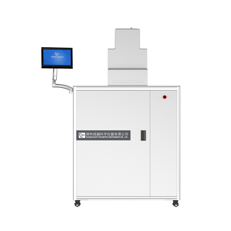

 system for Nanofilm")
 system for Nanofilm")

Plasma-Enhanced Atomic Layer Deposition (PEALD) combines the advantages of plasma and ALD to achieve higher film quality, lower deposition temperatures, and broader material compatibility. PEALD systems are widely used in microelectronics, optoelectronics, surface engineering, and other fields.

Plasma-Enhanced Atomic Layer Deposition (PEALD) combines the advantages of plasma and ALD to achieve higher film quality, lower deposition temperatures, and broader material compatibility. PEALD systems are widely used in microelectronics, optoelectronics, surface engineering, and other fields.
1.Plasma-Enhanced Reactions: PEALD uses plasma to excite reaction gases, enabling film deposition at lower temperatures, making it suitable for temperature-sensitive materials like organics or flexible substrates.
2.Higher Film Density and Purity: Plasma provides high-energy reactants, allowing the deposition of dense and pure films at lower temperatures, reducing defects and impurities.
3.Excellent Film Thickness Uniformity: Retains the ALD advantage of uniform film coverage on complex 3D structures and high aspect ratio substrates, essential for device miniaturization and nanostructure fabrication.
4.Flexible Process Control: Independent control of plasma generation and ALD precursor pulses offers great process flexibility. Plasma power, time, and gas flow can be adjusted to optimize deposition conditions for different materials.
5.Wide Material Compatibility: Suitable for depositing various materials, including oxides, nitrides, sulfides, and metals, and is particularly suitable for materials like SiNx, AlN, and TiN.
6.Low-Temperature Deposition: Compared to conventional thermal ALD, PEALD allows high-quality film deposition at lower temperatures, crucial for applications on temperature-sensitive substrates like polymers.
Model | CY-PEALD-150R |
Reaction chamber | The standard chamber can accommodate samples up to 6 inches in size with a maximum sample height of 6mm (optional customizations are available for extra tall samples as per user requirements). It features a DualOTM nitrogen-protected dual O-Ring high-temperature sealing system to prevent leakage of other gases. The substrate heating temperature is controllable from room temperature (RT) to 400°C, with a control accuracy of ±1°C. The chamber baking temperature is controllable from RT to 200°C, also with a control accuracy of ±1°C. |
Deposition mode | Includes the following three operating modes: High-speed deposition continuous mode TM (Flow TM) Deposition mode for ultra-high aspect ratio structures TM (StopFlow TM) Plasma-enhanced mode |
Precursor source | There are 5 precursor sources in total: 1 at room temperature and 4 heated sources. The heating temperature is controllable from room temperature (RT) to 200°C, with a control accuracy of ±1°C. The heated sources are equipped with high-temperature manual valves, and the standard precursor source bottle has a volume of 50cc. The room temperature source can be connected to water, ozone, oxygen, ammonia, H₂S, etc., for the preparation of oxides, nitrides, and sulfides. Any of the heated sources can be connected to the corresponding precursor sources. |
Precursor pipeline | All precursor pipelines are made of 316L stainless steel EP grade pipelines, and the heating temperature of all pipelines is controllable to RT-150°C. |
ALD valve | Each precursor is equipped with a high-speed and high-temperature ALD valve dedicated for atomic layer deposition; the ALD valve adopts system-integrated surface mounting and can be replaced by a blind plate during maintenance and replacement; the valve body heating temperature is controllable at RT-150℃ |
Vacuum gauge | Imported wide range vacuum gauge, measuring range 2x10⁻⁴ to 10+3torr. |
Exhaust pipe | The heating temperature of the exhaust pipe is controllable from RT to 150℃; equipped with a stop valve, the heating temperature is controllable from RT to 150℃. |
Ozone generator system | High concentration ozone generator, including pipelines and cracker accessories; maximum output >15g/h, power adjustable from 0 to 300W, maximum concentration >3.5% (w/w) |
Optional microwave plasma system | Automatically matched microwave plasma source system, which includes: Adjustable microwave power output from 0 to 200W. Ultra-fast plasma generator capable of achieving stable plasma ignition in as little as 200ms. There are 2 plasma sources: One source is equipped with a mass flow controller (MFC) for argon (Ar). The other source can supply pulse gases such as H₂, O₂, N₂, NH₃, H₂S, and can be switched as needed. |
Control hardware | PLC control system. |
Control software | autoALDTM special software fully automatically controls heating, flow, and other deposition processes, as well as real-time monitoring of temperature, pressure, etc. |
Vacuum pump | Mechanical pump |
Warranty | one year free warranty starting from the date of acceptance. |
Installation and training | On-site installation and training by engineers |
Name | Description |
Host | Standard 6-inch Atomic Layer Deposition (ALD) system includes: 5 precursor sources, including piping, high-temperature ALD valves, and 50ml source bottles, 4 heated sources and 1 room temperature source, Automated deposition control system, autoALDTM deposition program control software, A laptop pre-installed with Windows TM. |
Ozone generator system | High concentration ozone generator, including pipelines and cracker accessories Maximum output>15g/h, maximum concentration>3.5%(w/w) |
Optional microwave plasma source system | Automatically matched microwave plasma source system, which includes: Adjustable microwave power output from 0 to 200W. Ultra-fast plasma generator capable of achieving stable plasma ignition in as little as 200ms. There are 2 plasma sources: One source is equipped with a mass flow controller (MFC) for argon (Ar). The other source can supply pulse gases such as H₂, O₂, N₂, NH₃, H₂S, and can be switched as needed. |
Vacuum mechanical pump system | Mechanical pumps and related piping |
Application:
1. Semiconductor Manufacturing
High-k Dielectrics and Metal Gates: PEALD is used to deposit high-k materials (such as HfO₂, ZrO₂) and metal gate materials (such as TiN) in transistors, improving device performance and reducing leakage current.
Copper Interconnect Barrier and Liner Layers: PEALD can deposit low-temperature, high-quality barrier layers (such as TiN, TaN) to prevent copper diffusion in interconnect structures.
Passivation Layers: Depositing passivation layers in integrated circuits and other microelectronic devices to protect the device surfaces from environmental factors, thereby extending device lifespan.
2. Optoelectronic Devices
Solar Cells: PEALD is used to deposit passivation or buffer layers (such as Al₂O₃, ZnO) in thin-film solar cells (such as CIGS, CdTe, silicon-based solar cells) to enhance photovoltaic conversion efficiency and stability.
LEDs and OLEDs: Deposition of transparent conductive oxides (such as ZnO, SnO₂) or buffer layers in Light-Emitting Diodes (LEDs) and Organic Light-Emitting Diodes (OLEDs) to improve luminous efficiency and lifespan.
3. Nanotechnology
Nanostructure Coatings: PEALD can deposit uniform films on complex nanostructures (such as nanowires, nanotubes, quantum dots) to control their electrical, optical, and mechanical properties.
Nano device Fabrication: Provides precise material thickness control in the manufacturing of nanoscale electronic and photonic devices, making it suitable for creating ultra-thin functional layers.
4. Surface Engineering and Protective Coatings
Anti-Corrosion Coatings: Deposition of anti-corrosion coatings (such as Al₂O₃, TiO₂) on metal surfaces to enhance durability in corrosive environments, widely used in aerospace, chemical equipment, and other industries.
Biomedical Applications: Deposition of biocompatible coatings on implants and other biomedical devices to improve compatibility with human tissues and reduce rejection reactions.
5. Flexible Electronics
Flexible Displays: Low-temperature deposition of high-performance films for flexible displays (such as OLEDs, electronic paper), used in electrodes or protective layers.
Wearable Devices: Deposition of protective or functional layers to enhance the durability and performance of flexible and wearable devices.
6. Energy Storage and Conversion
Lithium-Ion Batteries: Deposition of protective layers on electrode materials (such as LiCoO₂, LiNiMnCoO₂) and electrolyte interfaces in lithium-ion batteries to extend battery life and improve charge/discharge performance.
Fuel Cells and Supercapacitors: Deposition of catalyst layers and protective layers to enhance the efficiency of fuel cells and the energy density of supercapacitors.
7. Sensor Technology
Gas Sensors: Deposition of functional films (such as ZnO, TiO₂) on the active or sensitive layers of sensors to improve detection sensitivity and selectivity for specific gases.
Biosensors: Deposition of functional films to enhance the recognition and detection capabilities of biosensors for target molecules.
8. Optical Components
Anti-Reflective Coatings: Deposition of anti-reflective coatings (such as SiO₂, Al₂O₃) on optical components to reduce light loss and improve transmittance, widely used in optical instruments and imaging devices.
Filters and Lenses: PEALD can deposit thin films with precisely controlled thicknesses for the fabrication of filters, mirrors, and other optical elements.
9. Display Technology
Thin-Film Transistors (TFTs): Used in the manufacture of thin-film transistors in Liquid Crystal Displays (LCDs) and OLED displays to improve resolution and performance.
Touch Screen Technology: Deposition of transparent conductive films (such as ITO, ZnO) in touch screens to enhance conductivity and durability.
Application Case (Depositing SiO₂ on PET Films):
The process of depositing silicon dioxide (SiO₂) on PET (polyethylene terephthalate) films using Plasma-Enhanced Atomic Layer Deposition (PEALD) technology requires careful attention to temperature control and plasma conditions to protect the temperature-sensitive PET material. The typical steps for depositing SiO₂ on PET films using PEALD are as follows:
1.Substrate Preparation
Cleaning the PET Film: Clean the PET film using an appropriate solvent (such as isopropanol or deionized water) to remove surface contaminants and organic residues. Gently wipe or use ultrasonic cleaning to ensure the surface is clean.
Drying the Substrate: Dry the PET film using nitrogen or dry air to ensure that no moisture remains on the surface.
2.Loading the Substrate
Fixing the PET Film: Place the cleaned PET film on the sample holder of the ALD system, ensuring that the film surface is flat and free from wrinkles.
Entering the Vacuum Chamber: Close the PEALD system’s sample chamber and evacuate it to the appropriate working pressure (typically between 10⁻³ and 10⁻⁵ Torr) to remove air.
3.Substrate Heating
Setting the Temperature: Due to the limited heat resistance of PET films, the temperature is usually controlled within a lower range (e.g., 50°C to 100°C) to avoid thermal damage to the film.
Stabilizing the Temperature: Wait until the substrate temperature is stable and evenly distributed across the film surface.
4.Depositing SiO₂ Thin Film
Pulse Precursor 1 (Silicon Source): Introduce silane (SiH₄) or tetraethoxysilane (TEOS) as the silicon source precursor. The precursor molecules adsorb onto the PET film surface.
Purge Step: Stop the flow of the silicon source precursor gas and clean the reaction chamber with an inert gas (such as argon or nitrogen) to remove any unreacted precursor molecules and by-products.
Plasma-Enhanced Reaction: Introduce oxygen (O₂) plasma. The plasma excites the oxygen molecules or atoms, which then react with the adsorbed silicon source precursor to form the SiO₂ thin film.
Plasma Conditions: Typically, a low-power plasma (e.g., 10-100 W) is used to avoid damage to the PET film.
Plasma Exposure Time: Set an appropriate plasma exposure time (usually a few seconds) to ensure uniform growth of the SiO₂ film.
Purge Step: Clean the reaction chamber again with an inert gas to remove residual reaction by-products, ensuring the formation of a pure SiO₂ film.
5.Repeating the Deposition Cycles
Number of Cycles: Repeat the "pulse silicon source - purge - plasma-enhanced reaction - purge" cycle according to the desired SiO₂ film thickness. Each cycle typically deposits about 0.1 to 0.2 nanometers of SiO₂ on the film surface.
Controlling Film Thickness: Adjust the number of cycles to control the final thickness of the SiO₂ thin film.
6.Cooling and Unloading
Cooling the Substrate: After deposition is complete, gradually reduce the reaction chamber temperature, allowing the PET film to cool to room temperature to avoid deformation or damage from sudden temperature changes.
Unloading the Substrate: Stop the deposition in a vacuum environment, restore the chamber to atmospheric pressure, and remove the deposited PET film.
7.Thin Film Characterization
Measuring Film Thickness: Use an ellipsometer or other thickness measurement equipment to check if the deposited SiO₂ film thickness meets expectations.
Surface Morphology Analysis: Examine the surface flatness and uniformity of the SiO₂ film using a Scanning Electron Microscope (SEM) or Atomic Force Microscope (AFM).
8.Post-Treatment (Optional)
Post-Annealing (if applicable): If needed, anneal the deposited SiO₂ film under suitable temperature conditions to improve film density and durability.
Notes:
Temperature Control: Maintain the deposition process temperature within the PET film’s tolerance range to avoid thermal damage or deformation.
Plasma Conditions: Use low-power plasma and optimize oxygen flow and plasma exposure time to minimize physical damage to the PET film.


Copyright © Zhengzhou CY Scientific Instrument Co., Ltd. All Rights Reserved Update cookies preferences
| Sitemap | Technical Support: 

 system for Semiconductor Manufacturing")