E-mail: cysi@cysi.wang

 system for Semiconductor Manufacturing")
 system for Semiconductor Manufacturing")

ALD systems are precise devices used for depositing ultra-thin films on substrates with atomic-level thickness control. They are commonly used in semiconductor manufacturing, nanotechnology, optoelectronics, and other high-tech fields

ALD systems are precise devices used for depositing ultra-thin films on substrates with atomic-level thickness control. They are commonly used in semiconductor manufacturing, nanotechnology, optoelectronics, and other high-tech fields.
Precise Thickness Control: ALD achieves atomic-level precision by introducing different precursor gases alternately, ensuring uniform film deposition.
Uniform Film Coverage: Capable of depositing films uniformly on complex 3D structures and substrates with high aspect ratios.
Material Compatibility: Can deposit various materials including oxides, nitrides, metals, and alloys.
High-Quality Films: Films produced are dense, defect-free, and have excellent electrical and mechanical properties.
Gentle Process Conditions: ALD processes are typically conducted at low temperatures, making them suitable for heat-sensitive materials.
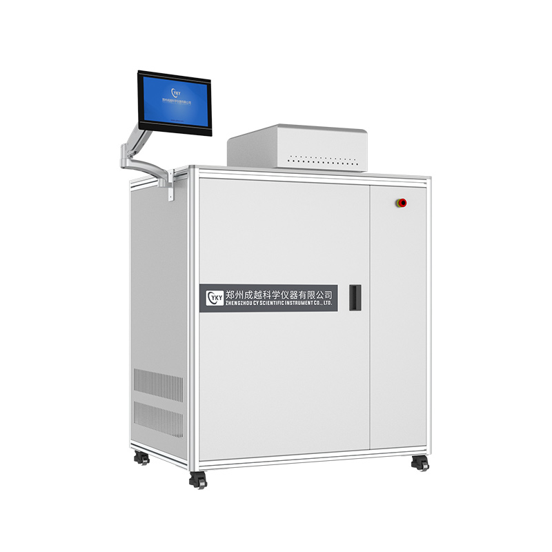
Model | CY-200S-ALD |
Reaction chamber | Standard chamber that can grow samples up to 8 inches, standard maximum sample height 20mm; (Super The high sample option can be customized according to user requirements and is optional), DualOTM nitrogen-protected dual O-Ring high temperature sealing system to isolate other gas leakage. Substrate heating temperature RT-400℃ available Control, control accuracy ±1℃; cavity baking temperature RT-200℃ controllable, control accuracy ±1℃ |
Deposition mode | Includes the following 2 working modes: Continuous mode TM for high-speed deposition (Flow TM) StopFlow TM for depositing ultra-high aspect ratio structures |
Precursor source | There are 5 precursor sources in total; 1 is a normal temperature source and 4 are heating sources. The heating temperature can be RT-200℃. control, with a control accuracy of ±1°C; the heating source is equipped with a high-temperature manual valve; the standard precursor source bottle has a volume of 50cc. Route 1 is a normal temperature source that can be connected to water/ozone/oxygen/ammonia/H2S source, etc. to prepare oxides, nitrogen compounds and sulfides. Any heating source can be connected to the relevant precursor source. |
Precursor pipeline | All precursor pipelines are made of 316L stainless steel EP grade pipelines, and the heating temperature of all pipelines is controllable to RT-150°C. |
ALD valve | Each precursor is equipped with a high-speed and high-temperature ALD valve dedicated for atomic layer deposition; the ALD valve adopts system-integrated surface mounting and can be replaced by a blind plate during maintenance and replacement; the valve body heating temperature is controllable at RT-150℃ |
Vacuum gauge | Imported wide range vacuum gauge, measuring range 2x10⁻⁴ to 10+3torr. |
Exhaust pipe | The heating temperature of the exhaust pipe is controllable from RT to 150℃; equipped with a stop valve, the heating temperature is controllable from RT to 150℃. |
Ozone generator system | High concentration ozone generator, including pipelines and cracker accessories; maximum output >15g/h, power adjustable from 0 to 300W, maximum concentration >3.5% (w/w) |
Upgrade interface | Upgrade interface for upgrading 6-channel precursor source; Hardware and software interfaces for in-situ upgrade of microwave plasma sources or molecular kinetic energy systems; The above upgrade interface can realize in-situ upgrade without returning the device to the manufacturer. |
Control hardware | PLC control system. |
Control software | autoALDTM special software fully automatically controls heating, flow, and other deposition processes, as well as real-time monitoring of temperature, pressure, etc. |
Vacuum pump | Mechanical pump |
Warranty | One year free warranty starting from the date of acceptance. |
Installation and training | On-site installation and training by engineers |
Name | Description |
Host | Standard 8-inch Atomic Layer Deposition System include: 5-way precursor source, including pipeline, high temperature ALD valve, 50ml source bottle, No. 4 is the heating source and No. 1 is the normal temperature source. Deposition automatic control system, autoALDTM deposition program control software, Laptops with Windows TM pre-installed, |
Ozone generator system | High concentration ozone generator, including pipelines and cracker accessories Maximum output>15g/h, maximum concentration>3.5%(w/w) |
Tall sample chamber cover | For loading high (suitable for high sample height ≤ 20 mm) samples |
Vacuum mechanical pump system | Mechanical pumps and related piping |
Application:
1.Semiconductor Manufacturing:
Gate Oxides: Used in the production of advanced semiconductor devices, such as Metal-Oxide-Semiconductor Field-Effect Transistors (MOSFETs).
High-k Dielectrics: Deposition of high dielectric constant materials in integrated circuits to enhance device performance and reduce leakage.
Copper Interconnects: Improvement of copper interconnect structures in semiconductor chips by depositing barrier layers and seed layers.
2.Memory Devices:
DRAM and Flash Memory: Deposition of high-k materials and conductive layers in Dynamic Random Access Memory (DRAM) and flash memory (e.g., 3D NAND) to enhance storage density and performance.
3.Optoelectronic Devices:
Solar Cells: Deposition of transparent conductive oxides or passivation layers in thin-film solar cells to enhance photovoltaic conversion efficiency.
LEDs and OLEDs: Deposition of emissive layers and electrode materials to improve the performance of Organic Light-Emitting Diodes (OLEDs) and Light-Emitting Diodes (LEDs).
4.Nanotechnology:
Nanostructure Coatings: Uniform deposition of thin films on complex nanostructures like nanowires and nanotubes to optimize optical and electrical properties.
Quantum Dot Coatings: Deposition of protective or functional thin films on quantum dot materials to enhance their stability and efficiency.
5.Protective Coatings:
Electronics: Deposition of moisture-resistant and corrosion-resistant coatings on electronic devices to extend their lifespan.
Medical Devices: Deposition of biocompatible coatings on biomaterials and implants to improve their compatibility with human tissues.
6.Catalyst Preparation:
Precise Catalyst Layers: Enhancement of catalytic performance by controlling the thickness and distribution of catalyst layers, widely used in chemical reactions and energy conversion.
7.Energy Storage:
Battery Electrodes: Deposition of thin film electrode materials in lithium-ion batteries and supercapacitors to increase energy density and cycle life.
Fuel Cells: Deposition of thin films on electrodes and proton exchange membranes in fuel cells to improve efficiency and durability.
8.Sensors:
Gas Sensors: Deposition of sensitive thin films on gas sensors to enhance their detection sensitivity and selectivity for target gases.
Biosensors: Deposition of functional thin films on biosensors to improve their ability to recognize and detect biomolecules.
9.Display Technology:
Thin-Film Transistors (TFTs): Used in the manufacture of thin-film transistors in Liquid Crystal Displays (LCDs) and Organic Light-Emitting Displays (OLEDs) to improve display performance.
Touch Screens: Deposition of conductive thin films in touch screens to enhance their electrical performance and touch sensitivity.
Application Case (Depositing Al₂O₃ on Silicon or Glass Substrates):
The process of depositing aluminum oxide (Al₂O₃) thin films on silicon or glass substrates using Atomic Layer Deposition (ALD) technology typically includes the following steps. This process primarily relies on the alternating introduction of precursors and reactive gases to achieve atomic-level film growth.
1.Substrate Preparation
Cleaning the Substrate: Clean the silicon or glass substrate thoroughly, typically using chemical cleaning methods to remove organic contaminants and particles. For silicon substrates, hydrofluoric acid (HF) etching may be performed to remove the surface oxide layer.
Drying the Substrate: Use nitrogen or other anhydrous gases to dry the substrate, ensuring that no moisture remains on the surface.
2.Loading the Substrate
Placing the Substrate: Place the cleaned silicon or glass substrate on the sample holder in the ALD system, ensuring that the smooth side is facing up.
Entering the Vacuum Chamber: Close the sample chamber of the ALD system and evacuate the air, typically reducing the chamber pressure to the range of 10⁻³ to 10⁻⁶ Torr.
3.Heating the Substrate
Setting the Temperature: Heat the substrate to an appropriate deposition temperature. For Al₂O₃ deposition, the temperature is usually between 150°C and 300°C, depending on the precursor used and the desired film quality.
Stabilizing the Temperature: Before starting the deposition, ensure that the substrate temperature is stable and evenly distributed.
4.Depositing Aluminum Oxide (Al₂O₃)
Pulse Precursor 1 (TMA): Introduce trimethylaluminum (TMA) as the aluminum source precursor. The TMA molecules react chemically with the substrate surface, adsorbing a single atomic layer. This process typically lasts a few seconds.
Purge Step: Stop the flow of TMA precursor gas and flush the reaction chamber with an inert gas (such as nitrogen or argon) for a few seconds to remove any unreacted TMA molecules and reaction by-products.
Pulse Precursor 2 (Water or Ozone): Introduce water vapor or ozone as the oxygen source precursor, which reacts with the adsorbed TMA layer to form Al₂O₃, releasing by-products (such as methane). This step also lasts a few seconds.
Purge Step: Again, flush the reaction chamber with an inert gas to ensure that only the desired Al₂O₃ thin film remains.
5.Repeating the Deposition Cycles
Number of Cycles: Repeat the above "Pulse TMA - Purge - Pulse Oxygen Source - Purge" steps according to the required film thickness. Each cycle typically grows about 0.1 to 0.2 nanometers of Al₂O₃ on the substrate surface.
Controlling Film Thickness: Adjust the number of cycles to control the total thickness of the aluminum oxide thin film.
6.Cooling and Unloading
Cooling the Substrate: After deposition is complete, reduce the reaction chamber temperature to allow the substrate to cool to room temperature.
Unloading the Substrate: Stop the deposition in a vacuum environment, restore the chamber to atmospheric pressure, open the chamber, and remove the deposited silicon or glass substrate.
7.Post-Treatment (Optional)
Post-Annealing: Depending on the application requirements, the deposited Al₂O₃ thin film may undergo heat treatment (such as annealing in an oxygen environment) to improve the film's physical and chemical properties.
8.Thin Film Characterization
Measuring Film Thickness: Use an ellipsometer or other thickness measurement equipment to check if the deposited Al₂O₃ film thickness meets expectations.
Surface Morphology Analysis: Examine the surface flatness and uniformity of the film using a Scanning Electron Microscope (SEM) or Atomic Force Microscope (AFM).


Copyright © Zhengzhou CY Scientific Instrument Co., Ltd. All Rights Reserved Update cookies preferences
| Sitemap | Technical Support: 

 system for Nanofilm")